
Huawei has introduced a new semiconductor development framework called the τ (Tau) Scaling Law, positioning it as a potential alternative to traditional transistor scaling as the semiconductor industry faces growing physical and economic constraints.
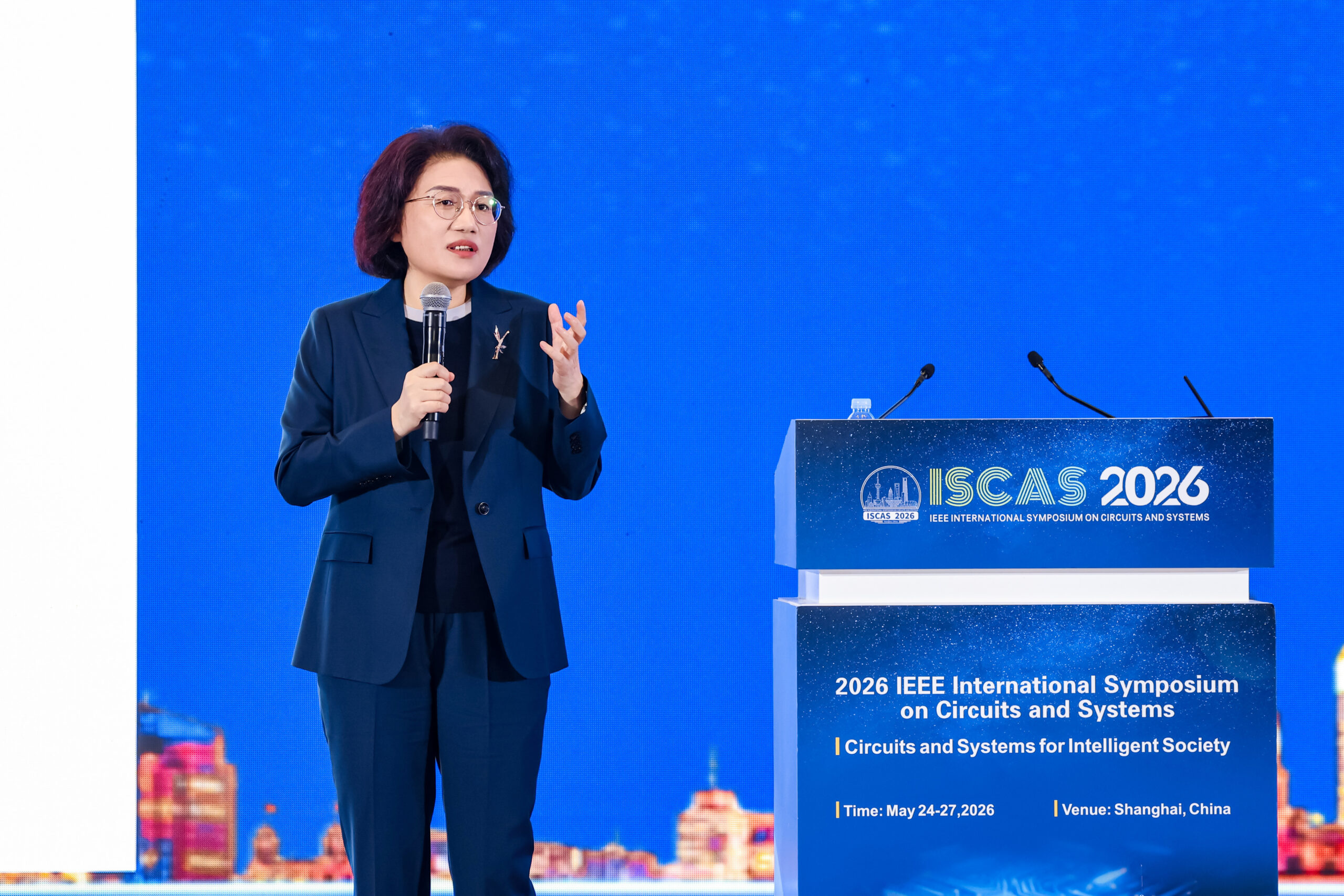
The concept was presented by He Tingbo, Director, Chair of Huawei Scientist Committee, ITMT Director, President of the Semiconductor Business, during a keynote speech titled “New Semiconductor Path in Practice” at the 2026 IEEE International Symposium on Circuits and Systems (ISCAS).
For decades, Moore’s Law has guided semiconductor progress through the continuous shrinking of transistor size. However, as manufacturing approaches advanced process limits, the pace of geometric scaling has slowed while development costs have increased significantly.
Huawei’s τ Scaling Law proposes shifting the industry’s focus from geometric scaling to time constant (τ) scaling. The framework is designed around reducing signal propagation delay across semiconductor devices, circuits, chips, and computing systems in order to improve performance, energy efficiency, and transistor density.
As part of this approach, Huawei introduced technologies including LogicFolding, a circuit architecture designed to shorten critical-path wiring and reduce latency, and UnifiedBus, an interconnect architecture aimed at reducing communication latency across computing systems.
The company said it has designed and mass-produced 381 chips over the past six years based on the τ Scaling Law framework. Huawei also stated that Kirin chips scheduled for launch in Fall 2026 will be the first to adopt the LogicFolding architecture.
According to Huawei, high-end chips developed under the framework are expected to achieve transistor density equivalent to 14Å (1.4nm) processes by 2031.
Looking ahead, He Tingbo noted, “We believe that openness and collaboration are key to driving ongoing progress in the semiconductor industry. No single company can independently find all the answers along the path of semiconductor evolution. With the τ Scaling Law, we look forward to working closely with scientists, engineers, and industry partners around the world to drive the sustainable development of the semiconductor and electronics industries.”








Discussion about this post